Lattice Semiconductor, today announced a Single Wire Aggregation (SWA) IP solution for reducing overall system size and BOM cost in industrial, consumer, and computing applications. The solution is a quick, easy, and innovative way for developers to use low power, small form factor Lattice FPGAs to dramatically reduce the number of board-to-board and component-to-component connectors in their embedded designs to increase reliability and reduce overall system footprint and cost.
The connectors used to link circuit boards and modules in electronic systems are costly, take up valuable space in devices with tight form factors, and over time can degrade and negatively impact system reliability. Routing signals between multiple connectors on space-constrained circuit boards can create design challenges that increase overall time-to-market.
“Developers are always looking for innovative ways to simplify and accelerate the development of embedded systems, while still maintaining the lowest BOM cost possible. Our new SWA solution meets all three of these needs by reducing the number of connectors in a system,” said Hussein Osman, Market Segment Manager, Lattice. “The solution is a strong fit for both novice and expert FPGA developers. Its pre-configured bitstreams help those new to FPGA-based design quickly configure an SWA application without requiring HDL coding experience, while the solution’s support for expanded parameterization makes it easy for FPGA experts to combine the Lattice SWA bitstreams with their own HDL code.”
Featuring the extremely low power and small size Lattice iCE40 UltraPlus™ FPGA, the SWA solution provides the hardware and software developers require to implement a single wire interface capable of aggregating multiple common I/O (I2C, I2S, UART and GPIO) data streams between components and circuit boards in a system. Lattice currently offers the following aggregated I/O configurations in pre-configured bitstreams for fast application prototyping.
Two I2S, an I2C peripheral, an I2C controller, and eight GPIO signals
Six I2C controller and two GPIO signals
One I2C controller and 12 GPIO signals
Three I2C controller, two I2C peripheral, and 15 GPIO signals
One I2S, one I2C controller, one I2C peripheral, and eight GPIO signals
Lattice customers requiring customized configurations can source them directly from Lattice technical support at no charge.
For more information, including how to purchase the SWA solution’s pre-configured bitstreams and hardware reference design, please visit: https://www.latticesemi.com/singlewire. The board is available for purchase at $249.00 from Lattice’s online store.
All registered trademarks and other trademarks belong to their respective owners. For more details, please visit Lattice official site.
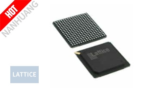
- IC FPGA 193 I/O 256FBGA
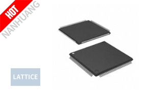
- IC FPGA 114 I/O 144TQFP
- IC FPGA 107 I/O 144TQFP
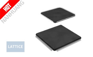
- IC CPLD 384MC 3.5NS 176TQFP
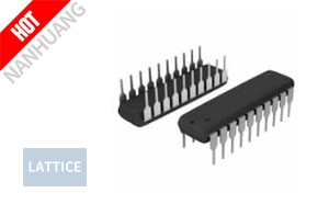
- IC CPLD 8MC 25NS 20DIP
- IC CPLD 64MC 12NS 48TQFP
- IP CORE 2D EDGE DETECTOR ECP2
- IC CPLD 32MC 5NS 44TQFP
- FIR FILTER GENERATOR ECP2 CONFIG
- IC FPGA 188 I/O 256FBGA
- IC VIDEO TRANSMITTER 100TQFP
- FPGA, 676 CLBS, 210000 GATES
- attice Semiconductor's iCE40 FPGA Enables Low Latency and Concurrent Sensor Processing in SteamVR Tr
- Lattice Expands Automate Solution Stack and Propel Design Tool Capabilities to Accelerate Industrial
- Lattice Named CES 2022 Innovation Awards Honoree
- Lattice Expands ORAN Solution Stack with Precision Timing and Secure Synchronization Support for 5G+
- Lattice Extends Product Portfolio with Introduction of CertusPro-NX FPGAs Optimized for Automotive A
- Lattice and LG Collaborate to Bring Edge AI Solutions to 2022 LG gram Premium Laptop Lineup
- Lattice Teams Up with Chromebook and Lenovo to Bring AI/ML Features to the Lenovo IdeaPad Flex 5i Ch
- Lattice Extends its Control FPGA Leadership with Introduction of MachXO5-NX Family
- Lattice Introduces ORAN Solution Stack to Accelerate 5G Customer Deployments
- Lattice Expands mVision Solution Stack with New Image Processing and Bridging Capabilities
- Lattice FPGAs Power Next Generation Lenovo Edge/AI Experiences
- Lattice Advances Industrial Automation at the Edge with Latest Solution Stack Updates


